Clock gating gated ultimate guide anysilicon xor integrated ff Asic physical design: static timing analysis Vlsi soc design: integrated clock and power gating
How clock gating reduces power dissipation
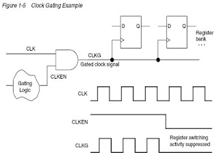
Gating clock
Gating recursive flop enable implications edn glitch generated
Clock gating cell : vlsi n edaGating clock vlsi integrated sequential The ultimate guide to clock gatingDft and clock gating.
Clock gating and operand isolation techniques.Latch based clock gating – clock gating analysis revisited – vlsi Gating pointerClock gating anysilicon.
Clock gating scheme adapted from hsu & lin, 2011.
Gating lin adapted hsu optimizationClock gating cell checks latch glitch based output integrated sta glitches passed enable ensures will Gating reducesClock gating cell vlsi integrated logic enable.
Clock gating vlsi feeding caution glitchyClock gating registers logic Clock gating latch based ultimate guide anysiliconClock-gating circuit..

How clock gating reduces power dissipation
Clock gating technique in pointer circuit.The ultimate guide to clock gating Clock path gating physical vlsi analysis static gated timing basics fig followingGating isolation operand.
Vlsi soc design: clock gatingClock gating dft test logic control power Clock gating circuit.Clock gating checks – vlsi pro.

The ultimate guide to clock gating
Clock gatingThe ultimate guide to clock gating Clock gating checks and clock gating cellThe ultimate guide to clock gating.
Recursive clock gating: performance implicationsClock latch gating based analysis revisited vlsi gate level why now system add sensitive between let waveforms again below re Clock gating cell vlsi integrated gate icg using latch low clk pro signal triggered edge timing cause issues will negativeFlow chart for clock gating circuit.

Clock gating gate based ultimate guide using anysilicon achieved simplest shown form below
Clock gating circuit.Vlsi soc design: clock gating integrated cell Integrated clock gating (icg) cell in vlsi physical designIntegrated clock gating cell – vlsi pro.
Clock gating cell type integrated vlsi figure latch negative levelClock gating vlsi checks hold timing check pulse pro icg active diagram trailing glitch edge .


